NSF IRES China 2017
Week 5
July 23rd 2017
Todsay was a rest day. Nothing eventful happened except naps and laundry.
July 24th 2017
As our fifth week began we started out hard at work in the lab. Today we spent our morning finishing our simulations and had our S Device code. By the time we left for lunch the S Device code was running smoothly, which was a huge relieve as that was a big portion of our research project since we would not be able to fabricate and test our own MOSFETs. After lunch, we worked on trying to change our S Device code so that it would take variable input. Although, this was not as particularly challenging as creating the SDE and S Device code, we had to make sure that we followed the rules established in Sentaurus when declaring and using variables in our codes. Therefore, by the end of the day we were able to have our code take numerical values from within the code itself, but also, take variable input designated by the user before allowing the code to run.
July 25th 2017
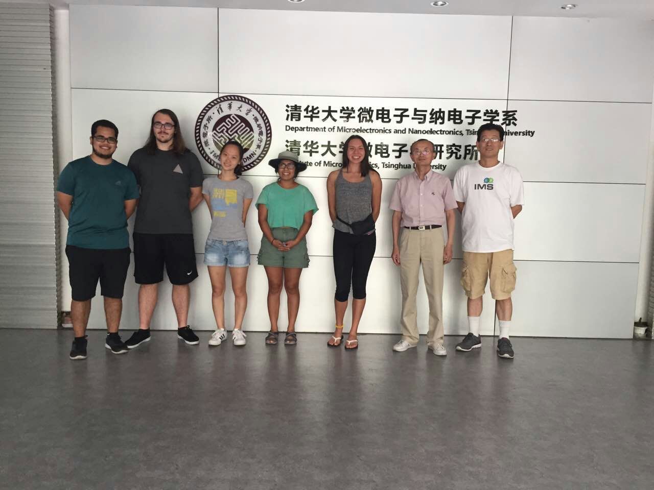
Today was another lab day. However, today was different from our usual routine since we finished our coding and simulations that would run on the computer. Today we received a PowerPoint to review on the actual fabrication process of a MOSFET. After lunch we met up with our host students Linyuan and Weijun and went over the PowerPoint they gave us, which allowed us to go more in-depth into the knowledge as well as confirm our own understanding of what we thought about the MOSFETs fabrication.
July 26th 2017
Another day was spent in the lab. Today we continued our discussion of the Powerpoint from yesterday, which was on the fabrication process of MOSFETs for both the morning and the afternoon, in preparation for going down into the clean room to observe some MOSFETs that our host students our working on. Today we mainly discussed about gate formation, drain/source formation, silicide formation, interconnected layers, and passivation.
July 27th 2017
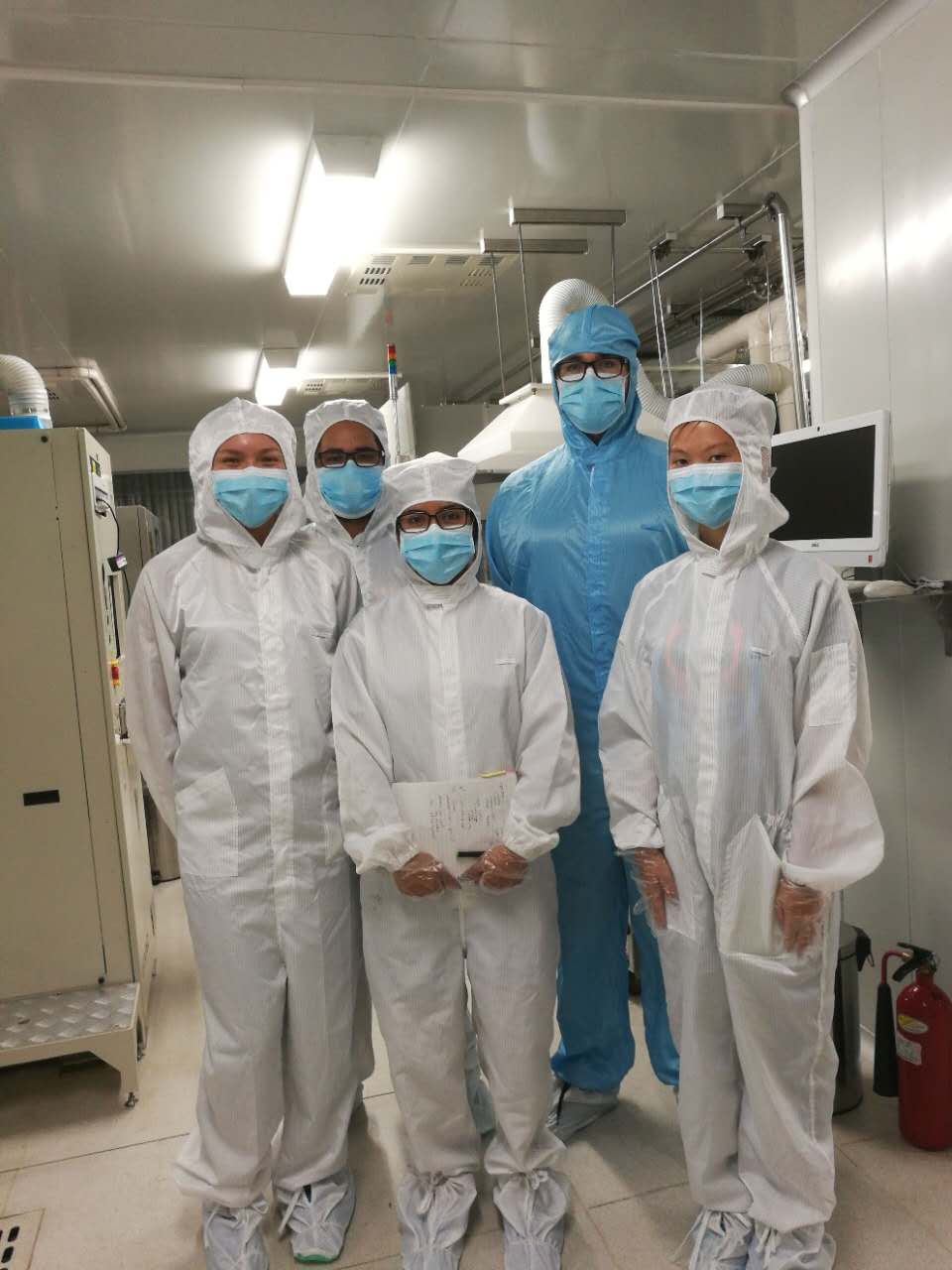
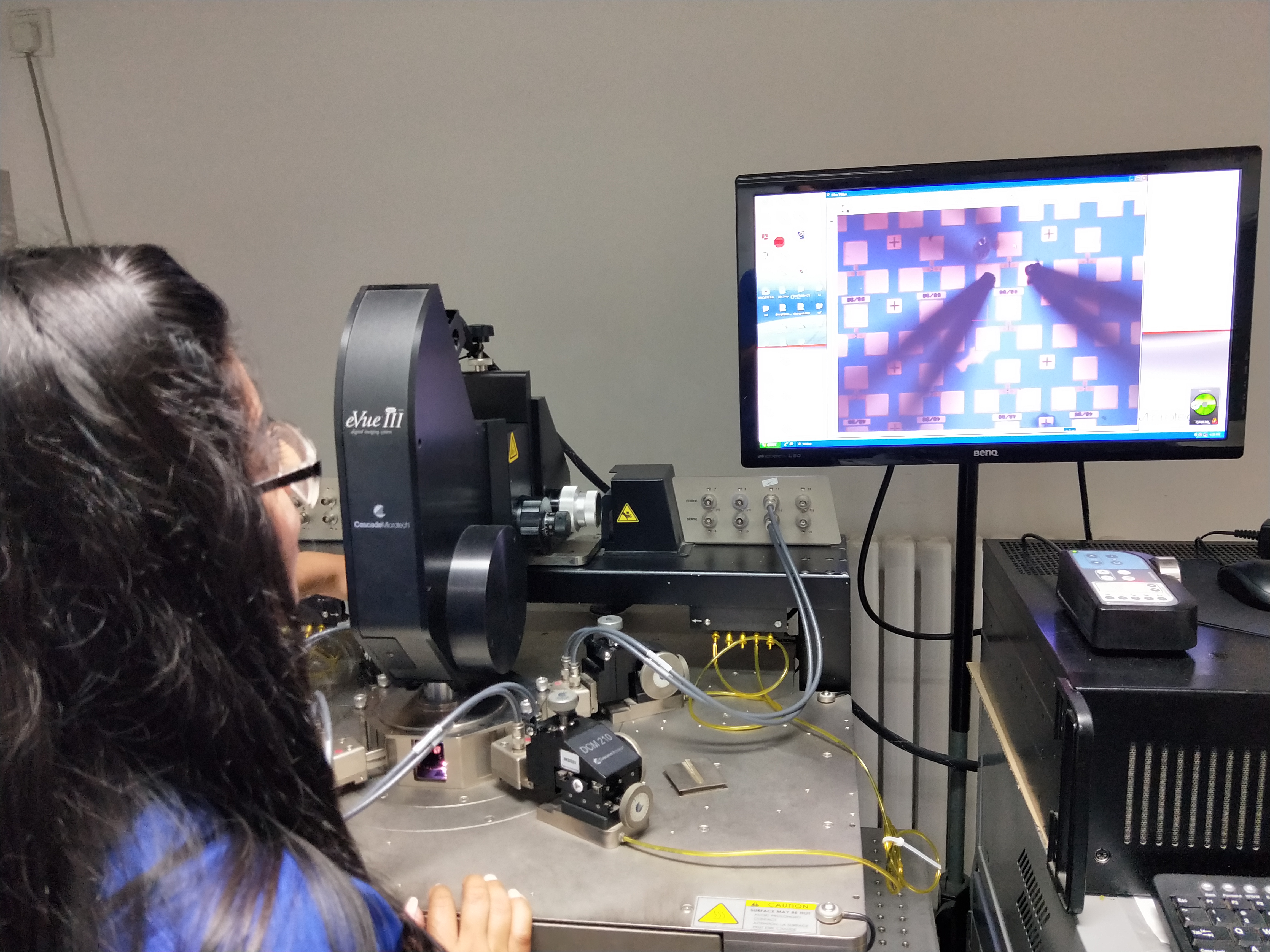
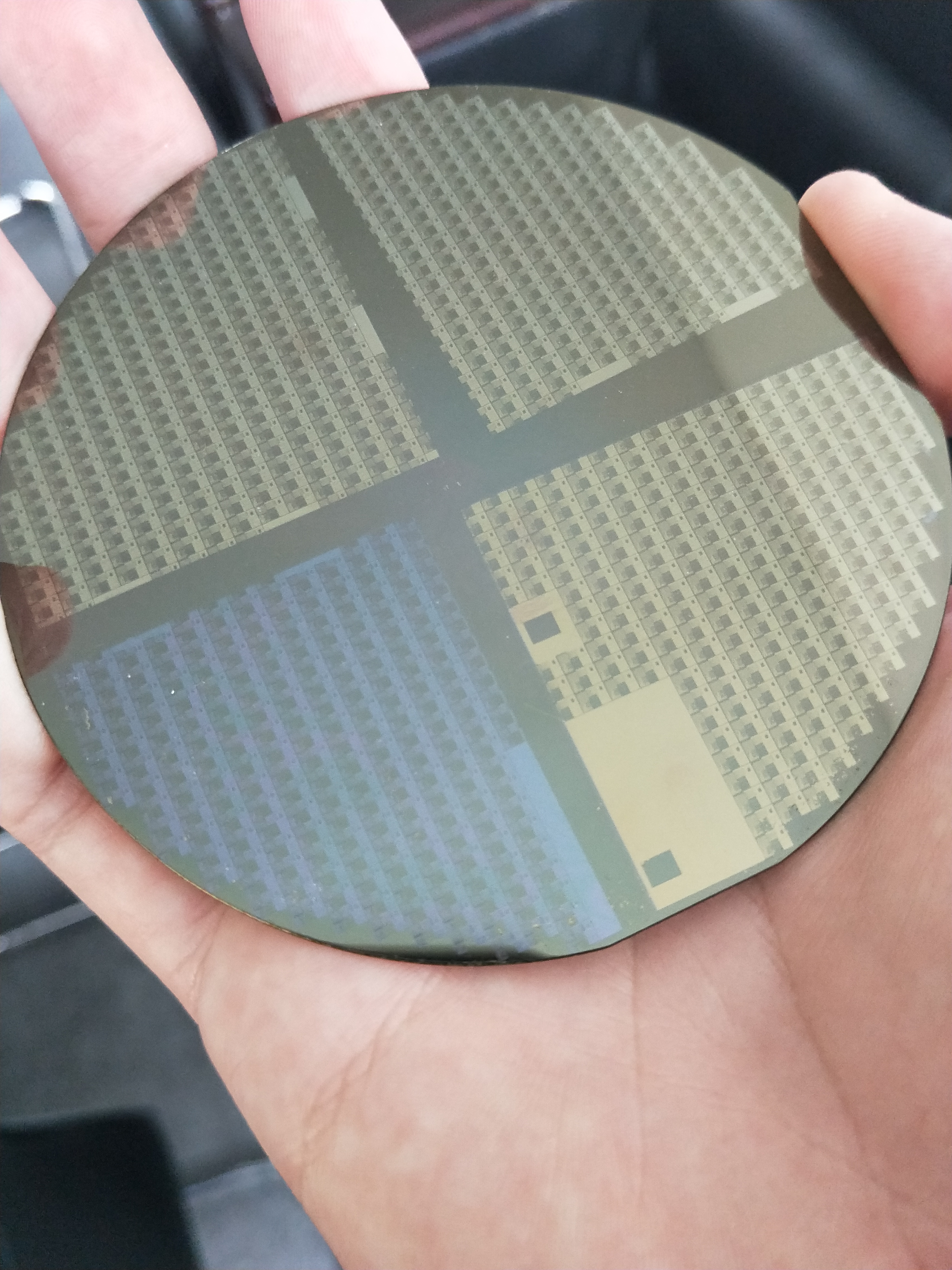
Today was an exciting day as we got to go into the clean room to actually see where the host students perform manipulations and fabrications of MOSFETs. All of us had to get into a full body lab suit, put on shoe covers, and wear masks in order to be able to go into the clean room. Before, we actually got into the room the last process to be cleared for entering was to take a high pressure “air shower” that removed and latent particles that may affect the experiments since they are on the Nano and Micro scale. Here, we got to learn how to clean MOSFET wafers using acids and pure water. We also, got to get an idea of what Moore’s Law really means as we got to see first-hand how many transistors are on a single wafer via a powerful microscope. Many of us got to see a Chemical Vapor Deposition machine as well as a scanning electron microscope for the first time as well. All in all it was a very eye opening experience to not only look at parts of the fabrication process but also get to see how the final product looks on the Micro and Nano scale.
July 28th 2017
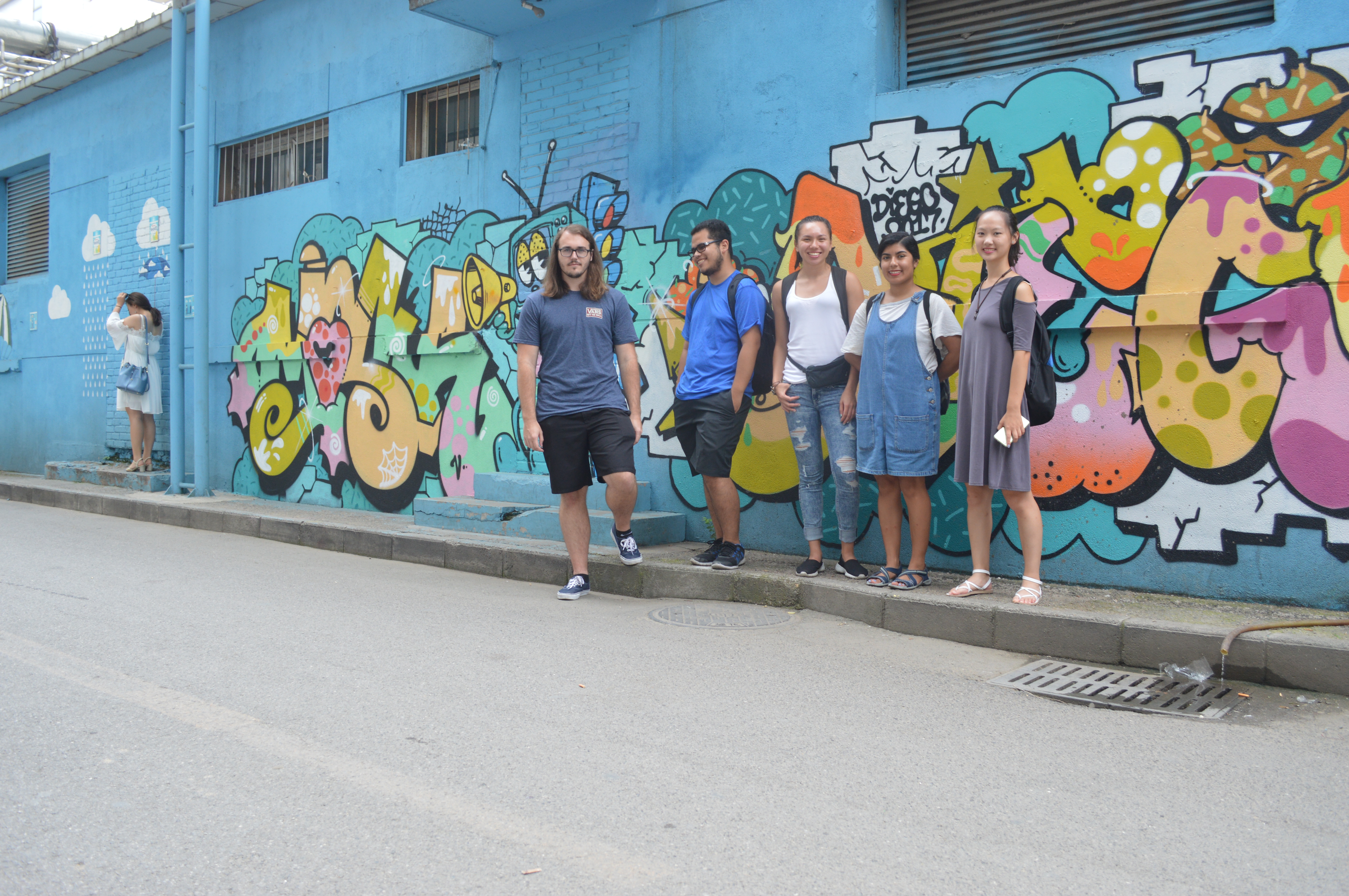
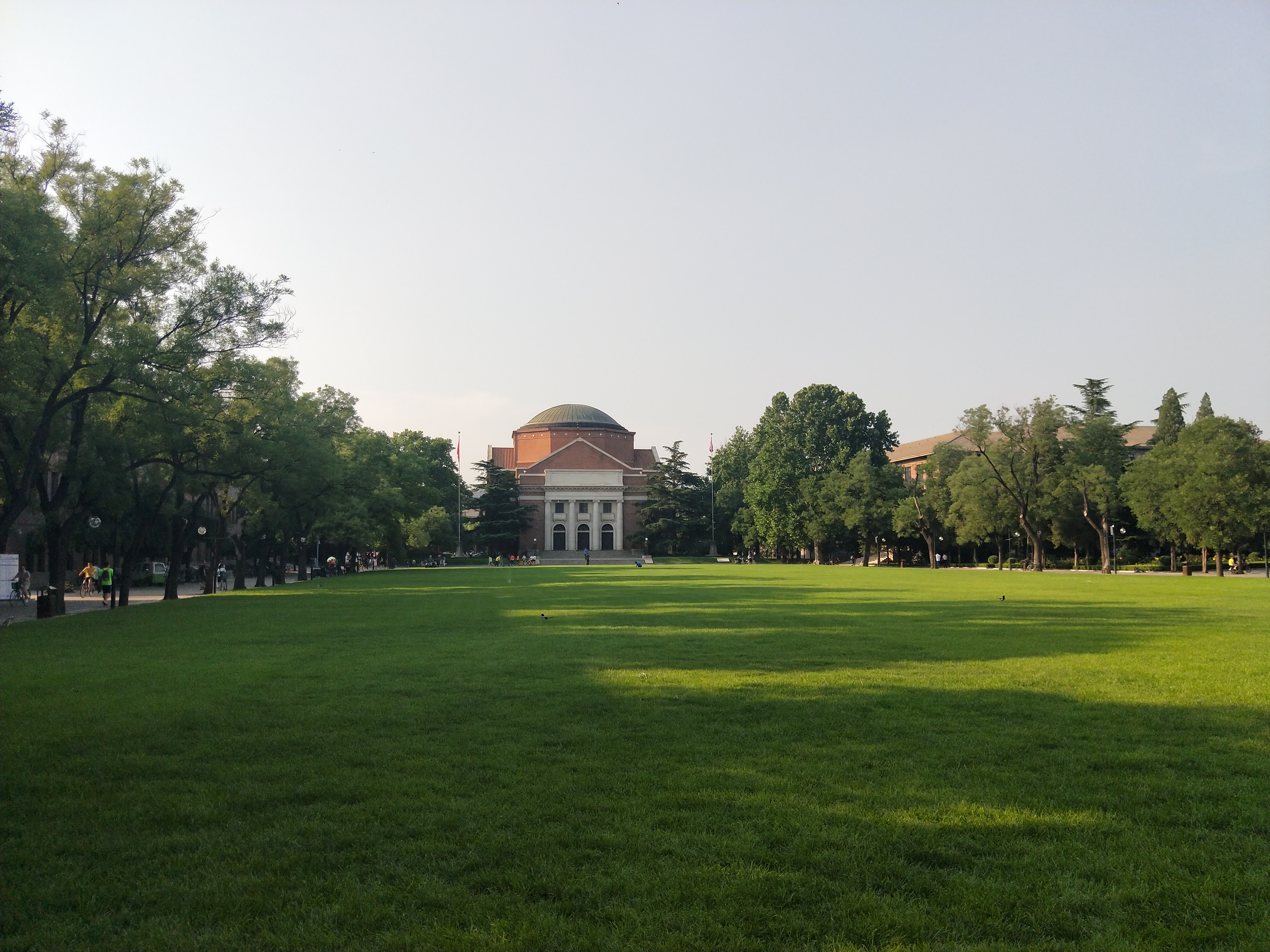
Today we got to relax after our long week in the lab. So, our adventure today took us to the Beijing Art District and we specifically went to part of the art district called 798. It was such an exciting experience to see the distinction between cultures, especially expressed in the art. What was interesting to note is that besides all the little shops there, most of the exhibition halls that we visited were converted from old factories so, it was a different atmosphere when looking at the art displayed and how the rooms were organized. For, lunch we went to a restaurant called Lakers, were we had an American style meal in which a majority of us ordered burgers and fries to sate our cravings for American food. Afterwards we continued to explore the art district and its shops till we arrived at an old train station that was converted into a restaurant and still had an engine from the past that looked to have been restored.
July 29th 2017
Today was a rest day