Apr 17th 2009 IEEE EDS DLs @ UCR
--------------------------------------------------------------------------------------------------
Nanotechnology Research Challenges for More Moore and Beyond
ABSTRACT
Since the invention of integrated circuit, scaling of devices in order to increase their performance has been following the well known Moore’s law. Nowadays, 32nm and below technologies are under development, while at device level the feasibility of 5nm geometries has been demonstrated. In addition, the convergence of these top-down technology, with bottom-up methods derived from fundamental disciplines such as materials physics, chemistry and biotechnology opens a totally new world of applications. Totally new type of devices, belong to the beyond-CMOS era, are gaining a lot of attention. Typical examples are carbon nanotubes, polymer electronics, spintronics, molecular electronics, etc. This lecture starts with a brief introduction on IMEC, before addressing the three main items of the Research Agenda, i.e., More Moore, Beyond CMOS and More than Moore. The main focus will be on nanotechnology for the More Moore and the Beyond-CMOS field. An overview will be given with emphasis on FinFETS, nanowires, carbon nanotubes (CNT), and graphene. These fields will be illustrated with research activities going on at IMEC.
 Prof. Cor Claeys received the
electrical-mechanical engineering degree in 1974 and the Ph.D. degree in
1979, both from the Katholieke Universiteit Leuven (KU Leuven),
effects, and defect engineering and material characterization. He authored two books, “Radiation Effects in Advanced Semiconductor Materials and Devices” and “Fundamental and Technological Aspects of Extended Defects in Germanium”, and edited two books, “Low Temperature Electronics” and “Germanium-Based Technologies: From Materials to Devices”. He also authored and co-authored eight book chapters and more than 800 technical papers. He has been involved in organizing of numerous international conferences and edited more than 40 Proceedings Volumes. He is an associated Editor for the Journal of the Electrochemical Society. He was Visiting Professor at the Queens University in Belfast, Ireland, and the University of Calabria, Italy. Prof. Claeys is a Fellow of IEEE and of the Electrochemical Society. He is current President for IEEE Electron Devices Society and an IEEE Distinguished Lecture since 2000. He received the IEEE Third Millennium Medal and the Electronics Division Award of the Electrochemical Society. He was elected as Academician and Professor of the International Information Academy.
-
From Millibits to
Terabits per Second and Beyond – 60+ Years of Innovation
ABSTRACT
The unfolding of the
Information Age has led to a plethora of products and services enriching our
lives and skyrocketing world economy. This advancement in telecommunications
has been driven by both hardware and software. The circuit complexity, as
portrayed by the number of transistors on the silicon chip, continues to
double every 24 months as pointed out by
 Dr.
Renuka P. Jindal received his Ph.D. degree in Electrical
Engineering from University of Minnesota in 1981. Upon graduation, he joined
Bell Laboratories at
-
Advanced
On-Chip ESD Protection Solutions in CMOS/BiCMOS Technologies
ABSTRACT
Electrostatic discharge (ESD) is a process in which a finite amount of charge is transferred from one object (i.e., human body) to the other (i.e., microchip). This process can result in a very high current passing through the microchip within a very short period of time, and more than 35% of chip damages can be attributed to such an event. As such, designing robust on-chip ESD structures to protect microchips against the ESD stress is a high priority in the semiconductor industry. An overview on the ESD sources, models, protection schemes, and testing will first be given in this talk. This is followed by the examples of robust ESD solution designs for protecting various CMOS/BiCMOS integrated circuits for digital and analog applications.
BIOGRAPHY
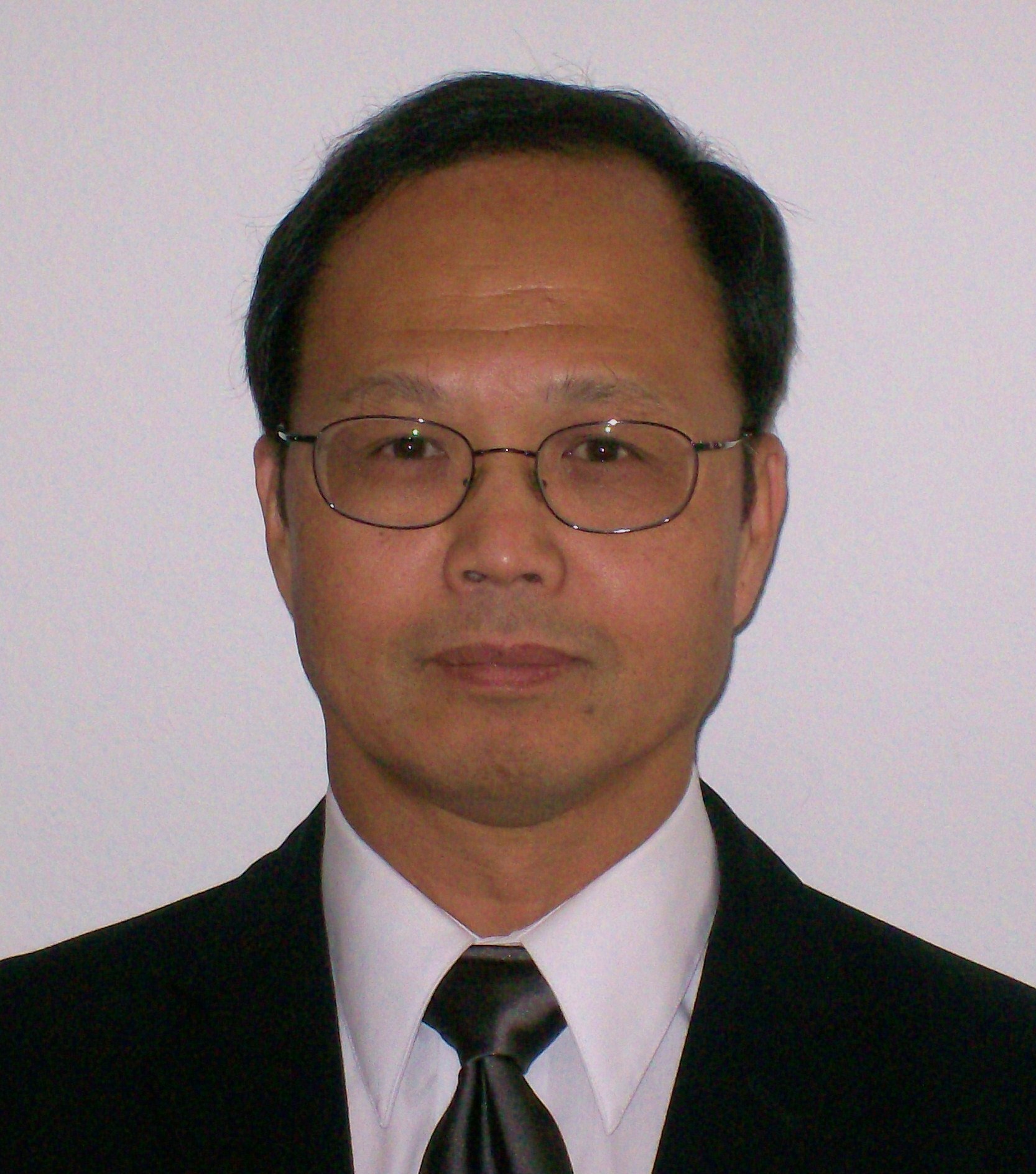
 Juin J. Liou
received the B.S. (honors), M.S., and Ph.D. degrees in electrical
engineering from the University of Florida, Gainesville, in 1982, 1983, and
1987, respectively. In 1987, he joined the Department of Electrical and
Computer Engineering at the University of Central Florida, Orlando, Florida
where he is now Analog Devices Professor. His current research interests are
Micro/nanoelectronics computer-aided design, RF device modeling and
simulation, and electrostatic discharge (ESD) protection design and
simulation. Dr. Liou has
published 8 books and more than 390 papers. His research has been sponsored
by various agencies (NSF, DARPA, Navy, Air Force, NASA, NIST, etc.) for more
than $9.0 Million. He is Editor for Microelectronics Reliability
journal. He served as General Chair or TPC
Chair for a large number of international conferences. Dr. Liou received ten
different awards on excellence in teaching and research from the University
of Central Florida (UCF) and six different awards from the IEEE Electron
Device Society including IEEE Joseph M. Biedenbach Outstanding Engineering
Educator Award in 2004. He is a Fellow of the Institute of Electronic
Engineers (IEE), an IEEE Distinguished Lecturer and an National Science
Council Distinguished Lecturer. He is Vice President for IEEE Electron
Devices Society. He holds several honorary professorships, including Yangtze
River Scholar Endowed Chair Professor – the highest honorary professorship
in China, NSVL Distinguished Professor, Chang Gung Endowed Professor of
Chang Gung University, Taiwan, Cao Guang-Biao Endowed
Professor of Zhejiang University, China, Consultant Professor
of Huazhong University of Science and Technology, Wuhan, China, and
Courtesy Professor of Shanghai Jiao Tong University, Shanghai, China. Dr.
Liou was a recipient of U.S. Air Force Fellowship Award and National
University Singapore Fellowship Award.
