2008 Report - Beijing
Introduction // Beijing // Chengdu // Conclusion
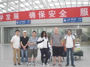
Arrival to Beijing
Once we had all arrived at Los Angeles International Airport, we realized we were all very excited and early! We all checked into Air China and sat down waiting to board. After boarding then sleeping through a 12-hour flight, we finally arrived at the Beijing Capital International Airport in the People’s Republic of China. We were taken aback by the size and grandeur of the building. Once there, we met up with two host students and Professor Wang from University of California, Riverside.
Figure B.1: Our host students received us
at the Beijing airport.
Before leaving the airport, we did not know what to expect with the weather, people or place. The moment we left the airport, we were hit with an explosion of heat. Luckily we quickly entered a van waiting for us and departed to our residence: Tsinghua University. We were not ready for the size of Tsinghua University. Once we arrived there, we all agreed we were completely lost. As the van made twists and turns and followed different road paths, we tried to keep but felt lost. Eventually we arrived at the Foreign Dormitories. That first day we accomplished so many tasks! We managed to register at Tsinghua University and receive our rooms. The rooms were completely identical and neatly arranged. There was a twin-sized bed, TV, closet, desk, telephone, sink and little bathroom. It was a perfectly sized one-person room. After depositing our suitcases in our rooms, we walked over to the bike lot and rented bikes. We were all excited to experience Chinese culture and immerse ourselves into the country. We felt that by doing what the Chinese did, we would fulfill our dreams that way.

Figure B.2: Riding our bikes with students
from our university in a different program.
Beijing Culture
Next we rode our bikes to obtain cafeteria cards. Fortunately for us, we were all extremely hungry by this time and since the cafeteria was close by, we simply walked over to it. We learned it was the oldest cafeteria in Tsinghua and considered small. We learned there were many more on the campus and some that were even four stories tall. We considered it a big cafeteria and were excited to see the dimension of the others. The cafeteria had many stationary chairs and tables where anyone could sit. Guests were meant to walk the stalls of food displayed by cafeteria workers behind windows and decide on what they wanted to eat. Once we all did, we sat down and enjoyed our first meal in China. We noticed that everyone there used chopsticks so those who did not know how to use them quickly learned that day. After the delicious meal, we visited a bank on campus to change our American Dollars into Chinese RMB. We were all able to change our money relatively quickly. After the stop at the bank, we left back to our rooms to rest until dinner.

Figure B.3: Learning how to use
chopsticks
When it was time for dinner, we all contacted each other on our room telephones and met downstairs. We happily rode our bikes to the restaurant where we met up with Professor Wang, and a new host student Jane. That night we ate traditional Peking duck and it was a consensus around the table that it was delicious! That night we experienced something new. We were impressed with the dinner style. The table had a spinning glass plate in the middle of the table where dishes were placed. If anyone wanted a dish on the other side of the table, they would spin the glass until the plate arrived in front of them. On top of the impressive table and beautiful surroundings, we tried completely new dishes we had never seen or heard of before. We left the restaurant happy and full and went to bed jetlagged but content and ready to familiarize us with China.
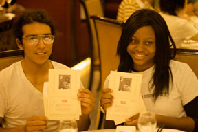
Figure B.4: Certificate of the ducks we had
for dinner
Assimilating Chinese culture
The next day we gained a better understanding of how vast the Tsinghua campus was. We rode our bikes around the campus and stopped at a phone shop so some of our members could obtain phones. We found that it was much cheaper to just buy a SIM card and put it in our American phones than to go through any other method. Once we completed our task there, we left to a student store to buy some necessary effects. We had learned in America that many public bathrooms did not have tissue paper so we made sure to buy some. We also bought other necessities such as bottled water, shampoo, and more. At the checkout stand, we were able to use our limited Chinese in trying to figure out the amount needed to be paid and give it. After leaving the student store, we truly realized how important our bikes where. Everyone at Tsinghua had a bike and there were bike locks and bike streets all around the university. We felt very thrilled to be a part of the university culture. We rode our bikes to the Main Building and were able to see where we would be doing our labs.
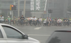
Figure B.5: Biking around Beijing
Sightseeing around Beijing
Fortunately we were able to find time outside of lab to travel the city. We were able to visit the Forbidden City, Tiananmen Square, old and new Summer Palaces, Wangfujing Plaza, Great Wall, China Central TV Tower and a Hutong and Tea House.
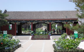
Figure B.6: Amazing architecture and
botanicals at the Old Summer Palace.
One of our favorite places was the Great Wall. When we went to visit the Great Wall, we underestimated how much walking we would do that day even though we knew the Great Wall winds up and down across deserts, grasslands, mountainvs and plateaus. Once we arrived, we were amazed at its beauty and immediately proceeded to walk up the wall and follow the path. Before arriving in China we learned that the Wall had been built as a defense but it had been destroyed in some parts and what we were seeing was mostly built in the Ming Dynasty.
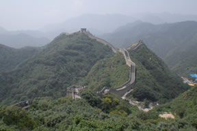
Figure B.7: Beautiful scenery at the Great
Wall
We also knew men had guarded these walls and if there was pending danger, a messenger had to run the stretch of the wall to proclaim the warning. What we did not know was how steep the wall could get at parts. We found ourselves breathing heavily and taking many breaks as we trekked the amazing world recognized monument. Once we reached high ground and were able to see our immense surroundings, we were fully able to appreciate the architecture and structure of the Great Wall. Unfortunately by the time we were all extremely tired so we decided to take a cable car to the bottom.

Figure B.8: Bright lights, signs and
paintings at Wangfujing
Wangfujing
Another favorite place we frequented was the Wangfujing Plaza. We met many other foreigners there who always wanted a rich experience of China. We visited the stores in that area and took in the beautiful lights and images there. After walking around for a while, we discovered a street in that area with a multitude of different foods. We walked down the whole street taking in the smells and admiring the brazen people eating the mysterious food. We loved Wangfujing Plaza because we were able to learn more about Chinese cuisine meet more Chinese as well as foreign people and have a good time doing so.
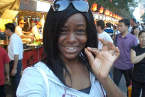
Figure B.9: Margaret trying unknown meat
The whole time spent in Beijing was informative, helpful and inspiring. We learned more than we thought we ever would about Chinese culture, food, architecture, hospitality and more. After a great time in Beijing, we were sad to leave but excited to visit a new city, Chengdu.
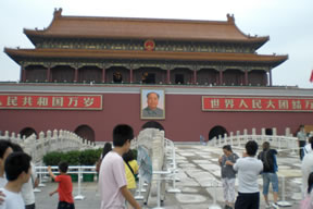
Figure B.10: Famous Mao painting at the
exit of Forbidden City
Seminar on Microelectronics at Tsinghua University by UC Santa Barbara Professor
As part of the activities organized by the IRES program, we had a speaker from the University of California, Santa Barbara, Professor Patrick Yue to talk about his research. We invited Tsinghua University students related to the field of Microelectronics to join us and we had a great response. We all learned about ongoing research at UCSB and, especially, at Dr. Yue laboratory, and the developments. After the seminar, there was an open time to ask questions about the research and related material to the field. We found this to be a great way to give something back to the host students and students in the department of Microelectronics. They seemed interested on what other people in the same field are working on. Also, they had the opportunity to ask questions about the challenges and possibilities to pursue their doctoral degree in an American Institution.
After the seminar was over, some of the students and us decided to go to lunch and have a good time, where we had more time to answer questions about how the higher level-school system works in America, if they ever decide to apply.

Figure B.11: Seminar on Microelectronics
at Tsinghua hosted by IRES program
Visiting SMIC semiconductor Foundry
Thanks to Dr. Wang’s networking with the Chinese industry, we were able to visit SMIC, Semiconductor Manufacturing International Corporation, foundry. We were well received by the people at SMIC. Before going in we had to wear covers for our shoes to prevent contamination of the actual clean rooms. First we were taken to a conference room, where an engineer and a human resources employee gave us a presentation about SMIC. At this presentation we learned that SMIC is one of the leading semiconductor foundries.
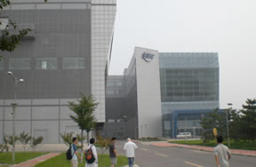
Figure B.12 On our way into SMIC
foundry
We learned that the company is headquartered in Shanghai, and has fabs in Tianjin, Beijing, Shanghai, and soon to be open, in Chengdu. The Beijing foundry has the technology to produced 12-inch wafers, the first of its kind in Mainland China. The integrated circuits technology that they produce ranges from 350 nm to 65 nm. We also had the opportunity to found out about the different companies that buy integrated circuits from SMIC to fabricate different components, such as, mixed signals/RF CMOS, high voltage, DRAM, flash, and EEPROM components, amongst others.
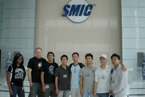
Figure B.12: At the main lobby of SMIC
Once the presentation was over, we had a tour around the foundry. We were not allowed to take any electronic devices because of confidentiality issues; nevertheless, it was an amazing experience. We got to see, how the massproduction of wafers is done, which is different from the way it is done at research level. We were truly amazed by the cutting edge technology that is used to mass-produce wafers. As we were walking around the foundry they mentioned us the incredibly large sum of money that is paid to open a foundry, which a huge portion of it, goes to buying the machines.
After visiting SMIC foundry we felt like we gain an insight on fabrication, as far as in the industry world. We found this really helpful because know we know the difference between how things are done in the industry and in research.
Laboratory at the Institute of Microelectronics, Tsinghua University
Tsinghua University is a university in Beijing, China. The university is internationally and nationally known as a top university in China. Its school of Information Science and Technology is highly prestigious because of its competitive program and research facilities. The IRES students were accepted as visiting students in the school of Information Science and Technology in the department of Microelectronics and Nanoelectronics in the program of Microelectronics and Solid State Electronics.
Our initial project, at Tsinghua University, was to design and fabricate semiconductor structures for RF and mixed-signal integrated circuits. But due to the Olympics activities, new government laws controlled the use of certain chemicals used in the fabrication of semiconductors. Nevertheless, we gain an insightful understanding about semiconductor design and measurement technologies used in the fabrication process of semiconductors.
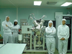
Figure B.13: Learning about the lab!
Getting to know the laboratory
We were all excited to visit the lab because we don’t have clean room facilities at our school. We learned that a clean room has a controlled level of contamination. In other words, it has a particular number of particles per cubic meter. This is vital in the manufacture of semiconductors.
We had to wear a jumpsuit that covered all our clothes and our head. Before going into the clean room we had to take an air shower. This shower is in between a double door connecting to the lab.
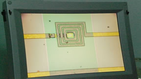
Figure B.14: An ongoing research on
capacitors on an integrated circuit
Integrated circuit fabrication process
Our host students walked us through the whole process of making a wafer. A wafer is a thin slice of semiconductor material used in the fabrication of integrated circuits. We learned about all the chemicals that are used in the process and their health risks if they’re not handle correctly. After this we went to the room where photolithography is done. This room uses ultraviolet light. Photolithography of a wafer works very similar to photography developing. You lay the wafer that you want your integrated circuit on, put the blue print on top of the wafer and turn on the aligner that emits light. The light only goes through where the blue print is not blocking the wafer.
After the wafer has been patterned using photolithography, etching is the next step. Etching removes layers from the surface of a wafer using chemicals. Etching entirely removes the top layer of a multilayer structure. This must be done without damaging the layers underneath.
We also learned about doping. Doping is a process where impurities are intentionally introduced into an extremely pure semiconductor. The reason this is important is to change the electrical properties of the semiconductor.
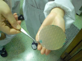
Figure B.15: Looking at different wafers

Figure B.17: MOSFET pad (Actual IC that
we tested)
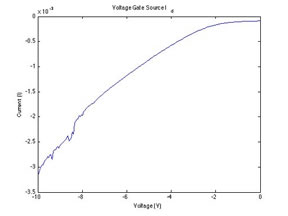
Figure B.16: Result for Drain current vs.
Voltage-Gate Source of a MOSFET
Testing MOSFETs and DIODES
As part of our lab activities we tested different MOSFETs. MOSFET (Metaloxide- semiconductor field-effect transistor) is a very common transistor used in both digital and analog circuits. The main purpose of this device is to amplify or switch signals. MOSFETs have three different operation modes, this are: cut-off mode, linear region, and saturation mode. Cut-off mode, according to the basic threshold model, means that the transistor is turned off, that is, there’s no current between the drain and source. MOSFET operation on the linear region means that the transistor is turned on. It basically operates like a resistor. In this region, the current is controlled by the gate voltage, this is proportional to the source and drain voltages. Saturation mode happens when the linear mode has been reached allowing the current to flow between the drain and source.

Figure B.9: Graph of MOSFET operating
in the linear region. Drain current vs.
Drain-to-source

Figure B.10 MOSFET #2 under testing.
Drain current vs. Voltage-Gate source

Figure B.11: MOSFET #2. Drain current
vs. Drain-to-source
In this part of the lab we learned how to use a pulse curve tracer, which traces the voltage through a circuit on a wafer. At first, we found this rather difficult because you need to look through a microscope in order to see the pads on the wafer. Moreover, it is even more challenging to get the probes to make good contact with the pads.
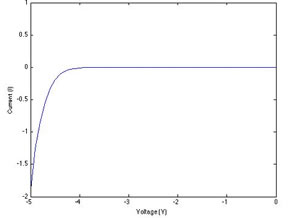
Figure B.12: I-V curve of a diode
operating on reverse bias

Figure B.13: I-V curve of a diode
operating on forward bias.
Once we got comfortable using the pulse curve tracer, we tested a diode on an integrated circuit. We tested this diode on the two operations: forward and reverse bias. We obtained the diode’s currentvoltage characteristic, also known as, I-V curve. Reverse bias operates on the third quadrant. It starts at infinity and approaches zero. As it approaches zero, the current is close to zero, this is known as breakdown. Forward bias operates on the first quadrant. It starts at zero, and the voltage and current start increasing, though the diode is off, but once it hits a certain voltage it turns on, allowing current to flow.
The next Figures show the different results we obtained from testing another diode.


Figure B.14 (a & b) Correspond to
Forward and Reverse Bias, respectively.
Modeling of a diode and MOSFET
As our last project in Beijing we had to model a diode and MOSFET using a computer program called Tonyplot. We had never used this program before, so it was a little difficult at the beginning. The most challenging part was to learn the commands Tonyplot uses. It was almost like learning a new programming language!
After debugging the code for a while and changing the parameters to meet our requirements we finally obtained models and simulations for our diode and MOSFET.
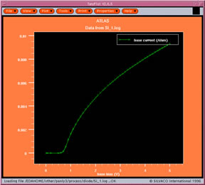
Figure B.12: Forward bias I-V
Characteristic (diode)

Figure B.13: Impurity levels of the diode
We learned how useful it is to model and simulate a device before it is manufacture. This helps rectify the theoretical analysis done, and gives you an idea of the characteristic you want to achieve on the actual device.

Figure B.14: Model and simulation of a
MOSFET. It shows the impurity levels and
the bandwidth of the MOSFET
After we finished with the lab activities in Beijing, we felt like we gained a profound understanding on the manufacture, simulation and testing of semiconductor devices. We think that what we learned in these sessions is going to be really helpful later on our career, because we will have a good understanding of semiconductors at the production level.
Introduction // Beijing // Chengdu // Conclusion
(c) 2009 University of Califronia, Riverside
Website Design by Cody Lewis